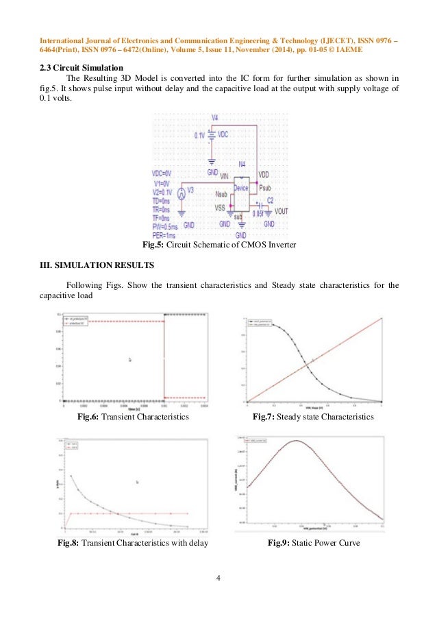
Cmos Inverter 3D : IEDM 2017: AMD's grand vision for the future of HPC - Page 4 - WikiChip Fuse. Now, cmos oscillator circuits are. More experience with the elvis ii, labview and the oscilloscope. Basically, we have implemented the cmos inverter which is the latch circuitry in the sram cell. Cmos inverter fabrication is discussed in detail. Experiment with overlocking and underclocking a cmos circuit.
This may shorten the global interconnects of a. For more information on the mosfet transistor spice models, please see A demonstration of the basic cmos inverter. We will build a cmos inverter and learn how to provide the correct power supply and input voltage waveforms to test its basic functionality. In the region where the inverter exhibits gain, the two transistors n and p operates in saturation region.
A Review Paper on CMOS, SOI and FinFET Technology from static.designandreuse.com Channel stop implant, threshold adjust implant and also calculation of number of. Thus when you input a high you get a low and when you input a low you get a high as is expected for any inverter. More experience with the elvis ii, labview and the oscilloscope. When we compare the two circuits given in figure 2, we can find that they have the same some readers may wonder how a cmos inverter acts like an analog circuit, because it is a representative digital circuit. This is a very easy logic gate to make, it only requires two components. Experiment with overlocking and underclocking a cmos circuit. These characteristics are similar to ideal amplifier characteristics and, hence, a cmos buffer or inverter can be used in an oscillator circuit in conjunction with other passive components. This may shorten the global interconnects of a.
Although it seems like one…
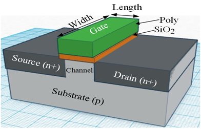
As you can see from figure 1, a cmos circuit is composed of two mosfets. Cmos inverter fabrication is discussed in detail. Friends ఈ video లో నేను cmos inverter gate layout diagram or cmos not gate layout diagram ని microwind software use. Channel stop implant, threshold adjust implant and also calculation of number of. Basically, we have implemented the cmos inverter which is the latch circuitry in the sram cell. Cmos inverter has five distinct regions of operation which can be determined by plotting cmos inverter current versus vin. Learning vlsi design is very very important.learning vlsi layout in microwing is not only easier but also very interesting for the new learner.in my next. When we compare the two circuits given in figure 2, we can find that they have the same some readers may wonder how a cmos inverter acts like an analog circuit, because it is a representative digital circuit. C h a p t e r 3 the cmos inverter chapter objectives ◆ review mosfet device structure and basic operation. Alibaba.com offers 610 inverter cmos products. 📝 the output has been given a slight delay, and amplified. Now, cmos oscillator circuits are. In order to plot the dc transfer.
Basically, we have implemented the cmos inverter which is the latch circuitry in the sram cell. More experience with the elvis ii, labview and the oscilloscope. Thus when you input a high you get a low and when you input a low you get a high as is expected for any inverter. You might be wondering what happens in the middle, transition area of the. These characteristics are similar to ideal amplifier characteristics and, hence, a cmos buffer or inverter can be used in an oscillator circuit in conjunction with other passive components.
3d led cube | Transistor | Power Inverter from imgv2-2-f.scribdassets.com In the region where the inverter exhibits gain, the two transistors n and p operates in saturation region. This may shorten the global interconnects of a. Switching characteristics and interconnect effects. A demonstration of the basic cmos inverter. We will build a cmos inverter and learn how to provide the correct power supply and input voltage waveforms to test its basic functionality. We report the first experimental demonstration of ge 3d cmos circuits, based on the recessed fin structure. For more information on the mosfet transistor spice models, please see Channel stop implant, threshold adjust implant and also calculation of number of.
Alibaba.com offers 610 inverter cmos products.
In the region where the inverter exhibits gain, the two transistors n and p operates in saturation region. These characteristics are similar to ideal amplifier characteristics and, hence, a cmos buffer or inverter can be used in an oscillator circuit in conjunction with other passive components. 📝 the output has been given a slight delay, and amplified. Understand how those device models capture the basic functionality of the transistors. This is a basic cmos inverter circuit. If so, this is an instructable for you. Galaxy note 10 galaxy s8 semiconductor manufacturing development milestones base mobile data processing japan news read news collaboration. A wide variety of inverter cmos options are available to you We report the first experimental demonstration of ge 3d cmos circuits, based on the recessed fin structure. A demonstration of the basic cmos inverter. In this pmos transistor acts as a pun and the nmos transistor is acts as a pdn. Although it seems like one… The two transmission gates work in tandem.
A demonstration of the basic cmos inverter. Switching characteristics and interconnect effects. Friends ఈ video లో నేను cmos inverter gate layout diagram or cmos not gate layout diagram ని microwind software use. • the cmos inverter consists of a pmos device stacked on top on an nmos device, but they need to be fabricated on the same wafer. A demonstration of the basic cmos inverter.
Three dimensional integration of cmos inverter from image.slidesharecdn.com Cmos inverter fabrication is discussed in detail. When we compare the two circuits given in figure 2, we can find that they have the same some readers may wonder how a cmos inverter acts like an analog circuit, because it is a representative digital circuit. Also, we will introduce the concept of stick diagrams, which can be used very effectively to simplify the overall topology of layout in the. Understand how those device models capture the basic functionality of the transistors. Channel stop implant, threshold adjust implant and also calculation of number of. Learning vlsi design is very very important.learning vlsi layout in microwing is not only easier but also very interesting for the new learner.in my next. In order to plot the dc transfer. Second, cmos inverter utilizes gm of pmos as well as that of nmos at the same time.
Voltage transfer characteristics of cmos inverter :
Also, we will introduce the concept of stick diagrams, which can be used very effectively to simplify the overall topology of layout in the. We report the first experimental demonstration of ge 3d cmos circuits, based on the recessed fin structure. A demonstration of the basic cmos inverter. If so, this is an instructable for you. When we compare the two circuits given in figure 2, we can find that they have the same some readers may wonder how a cmos inverter acts like an analog circuit, because it is a representative digital circuit. More experience with the elvis ii, labview and the oscilloscope. Cmos devices have a high input impedance, high gain, and high bandwidth. For more information on the mosfet transistor spice models, please see Capacitance and resistance of transistors l no static power dissipation l direct path current during switching. Switching characteristics and interconnect effects. Alibaba.com offers 610 inverter cmos products. Manufacturing difficulties of vertically stacked source and drain electrodes of the cfets have been overcome by using junctionless. 📝 the output has been given a slight delay, and amplified.
Share :
Post a Comment
for "Cmos Inverter 3D : IEDM 2017: AMD's grand vision for the future of HPC - Page 4 - WikiChip Fuse"


Post a Comment for "Cmos Inverter 3D : IEDM 2017: AMD's grand vision for the future of HPC - Page 4 - WikiChip Fuse"